Probe Card Solution
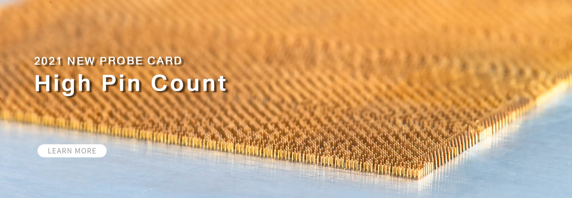
CHPT probe card solutions are suitable for market applications, such as the application process of mobile phones, high-performance computing, network, etc. Our probe cards have been verified for use by several global semiconductor firms.
Advantages of CHPT Probe Card
- CHPT probe cards have smaller scrub marks.
- Probe card life is confirmed to 1 million touchdowns.
- Compared to cantilever probe card, MEMS probe cards require less demanding in-house maintenance.
- We provide “All in House” service for our customers.
PCB Technology
High aspect ratio is the ratio value of board thickness and the aperture. CHPT normal PCBs reach 24 to 32 layers, and advanced PCBs are around 40 to 50 layers. The critical technologies for high aspect ratio include lamination, drilling and through-hole plating. With the increasing need for board thickness by semiconductor firms, the three technologies listed above have become more crucial across the industry.
a. Lamination
Precisely measure and calculate the basal lamina sizing of each layer using special riveting technology to make inner-layer registration reach the minimum shift.
▼ Accurately align and position layers together
b. Drill
In the PCB manufacturing process, there are two drilling processes, such as mechanical drilling, and laser drilling. Mechanical drilling is used to drill through holes. If the hole exceeds the limitations of the mechanical drill, we may use laser drilling.
c. Plated Through Hole (PTH)
The plating technology of precisely measured high aspect ratio is designed to achieve the highest processing ability in the industry. With a pitch that is 0.4 mm or above and an aspect ratio of 41, the maximum PTH copper thickness can reach to 1.0 mil.
| Pitch(mm) | Hole Size(mm) | Aspect Ratio | Min. Hole Copper Thickness(mm / mil) | Max. Hole Copper Thickness(mm/mil) |
|---|---|---|---|---|
| 0.32 | 0.125 | 40 | 0.01 / 0.4 | 0.015 / 0.6 |
| 0.35 | 0.125 | 40 | 0.01 / 0.4 | 0.015 / 0.6 |
| 0.40 | 0.150 | 41 | 0.01 / 0.4 | 0.025 / 1.0 |
| 0.50 | 0.200 | 40 | 0.01 / 0.4 | 0.025 / 1.0 |
Substrate Technology
The package technology is evolving in recent years, from Wire Bond to 3D IC. The IC Bump will be an inevitable trend. The advancement of packaging technology has influenced the development of the following technologies.
- Shrinking IC size
- Bump pitch keeps decreasing
- Improvement for IC complexity
- Signal transmission speed is increasing
When shrinking the IC bump we run into two main obstacles. One is reducing the drill size and another is decreasing the line width/pitch. The current measured technology can reach 20um of fine pitch and fine line.
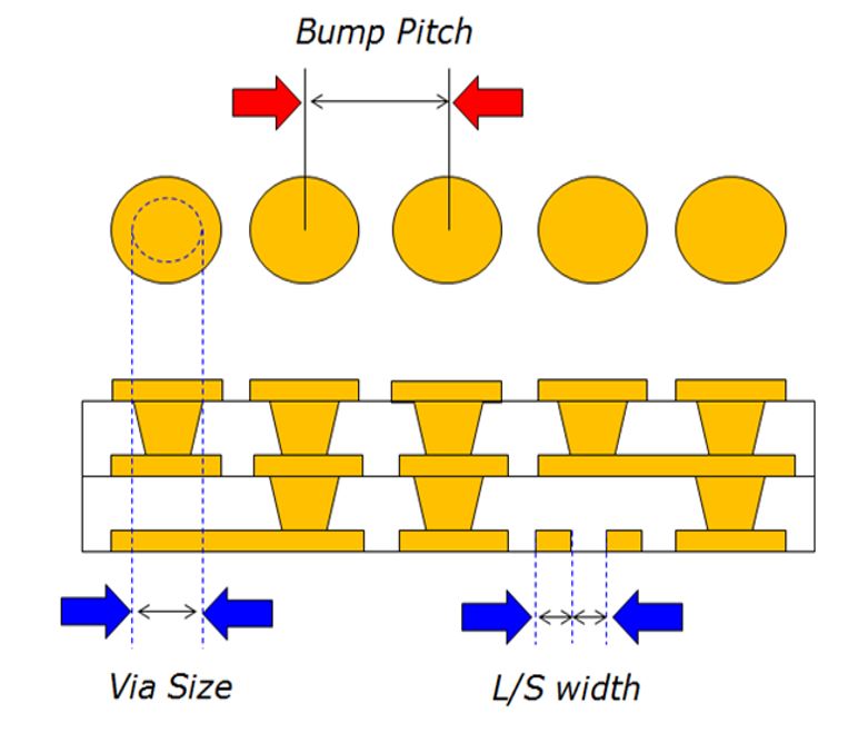
More wiring spaces are provided by Line/Space reduction. This not only reduces the number of layouts but also makes the design for Multi-DUT tests possible. Moreover, the shortening of the signal transmission route will be beneficial to the signal quality. CHPT has 50um pitch mass production experience. In addition to the 25um set aperture and the set Line/Space 20um/20um, the testing project can be made to correspond to the process level test for 10nm wafers.
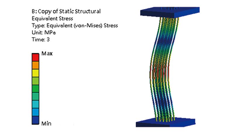
Probe Head Technology
CHPT has its own technology for developing and producing probing needles, and provides the standard needles that are open for customization. The metal composition of the raw materials can be adjusted according to the customer’s test conditions to produce high-performance needles that meet the customized requirements. Each probing needle goes through rigorous thermal cycle testing for reliability verification.
There are three series of probe head needles available for CHPT’s probe card solution. Each series of needles can be applied to high-speed computing, mobile phone technology, AIoT, and display.
● SR Series
SR series probing needles are tailor-made for high-performance computing chips with a bump/pad pitch of 90um, featuring an operation temperature of up to 150℃, frequency range up to 23GHz, and a maximum current per needle of 1500mA.
● BR Series
BR series probing needles are specially designed and developed for high-performance computing chips and RF chips with a bump/pad pitch of 130um to 180um, featuring an operating temperature of up to 150℃, frequency range up to 24GHz, and a maximum current per needle of 1500ma to 1800mA. They are also suitable for APU, GPU, and CPU chips.
● NS Series
NS series probing needles are designed and developed for AP, ASIC, TDDI, and modem chips. This series of needles has the combined characteristics of low force, high CCC, and a long lifetime. They are suitable for high-speeds up to 10 Gbps and a single-pin maximum current of 1200mA. NS series probing needles provide an excellent cost-performance ratio.
- Copyright © Chunghwa Precision Test Tech.Co., Ltd . All rights reserved.
- 中華精測科技股份有限公司 著作權所有