Aspect Ratio Max.: 47
Layer Count Max.: 100
Pitch Min.: 0.32mm
WAFERTEST (FT)
YesICAn important test interface after packaging, mainly serving as a carrierICAs a carrier, when the wafer undergoes processes such as dicing, die attach, and wire bonding, and is then encapsulated with materials like plastic, ceramic, or metal, yield testing must be performed again.
ICTest boards are mainly used inICPost-packaging yield test(Final Testing, FT)to perform functional testing and sorting, with the purpose of ensuringICwhether attributes such as functionality, speed, reliability, and power consumption are normal. Through testing at this stage, defective functions are eliminated.ICto further ensureICproduct quality, preventing the end product fromICDefects result in scrap,ICTest boards, like wafer test boards, can reduce waste in downstream process costs.

-
-
-
-
-
-
-
-
- PCIe G5 32 Gbps
- SerDes PAM4 112 Gbps
- High temperature, up to 125℃
- Suitable for pitch 650~ 1,000 μm
-
-
-
-
-
-
-
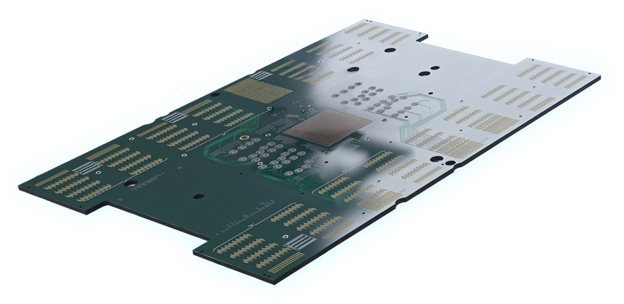
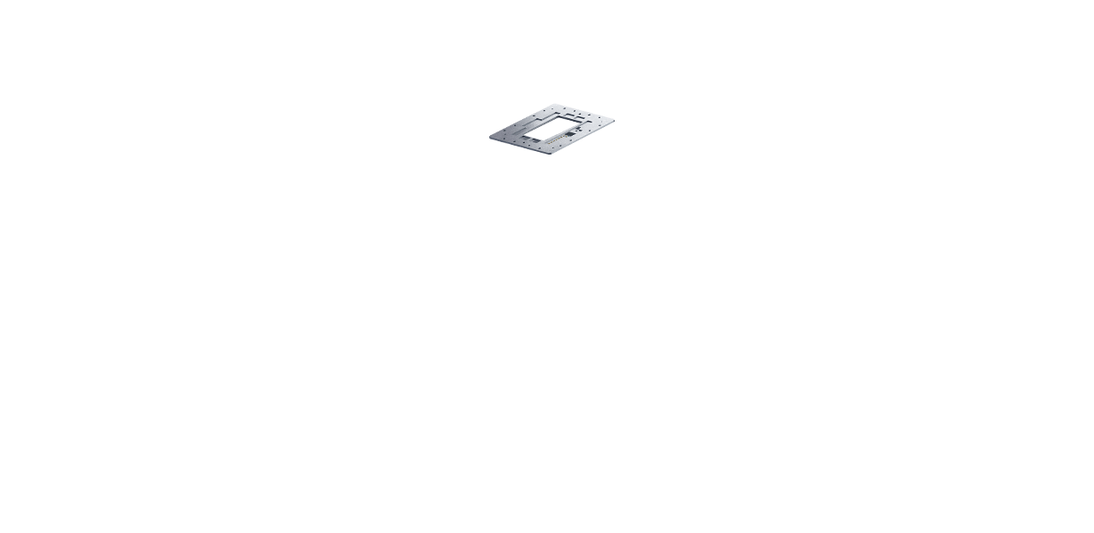
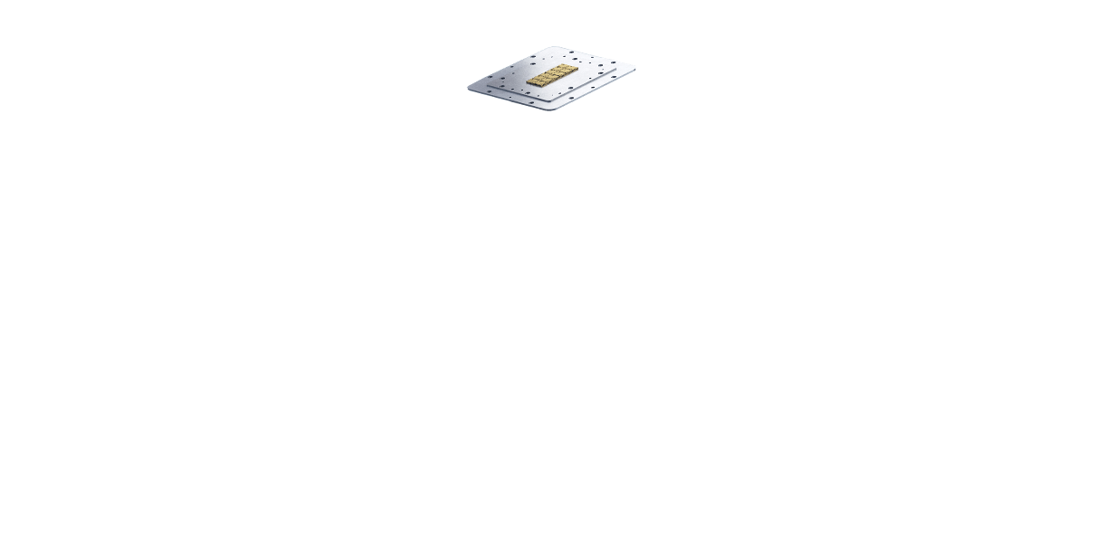
Probe card circuit board
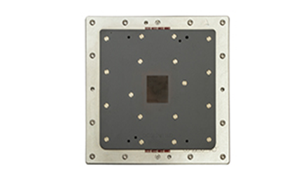
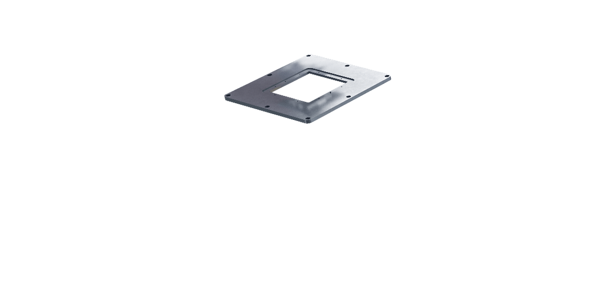
Probe tip
針頭類型:MEMS
針頭系列:NS、BKS、BR、SS
最大針腳數:50,000
針頭系列:NS、BKS、BR、SS
最大針腳數:50,000
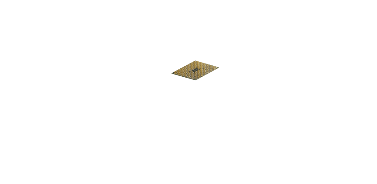
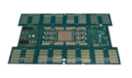
IC substrate
C4 Pad Count Max.: 50,000 pins
C4 Pad Pitch: 50-200um
ST Type: AMLO, TFMLO
C4 Pad Pitch: 50-200um
ST Type: AMLO, TFMLO
Probe card circuit board
Aspect Ratio Max.: 47
Layer Count Max.: 100
Pitch Min.: 0.32mm
Layer Count Max.: 100
Pitch Min.: 0.32mm
Probe tip
針頭類型:MEMS
針頭系列:NS、BKS、BR、SS
最大針腳數:50,000
針頭系列:NS、BKS、BR、SS
最大針腳數:50,000
IC substrate
C4 Pad Count Max.: 50,000 pins
C4 Pad Pitch: 50-200um
ST Type: AMLO, TFMLO
C4 Pad Pitch: 50-200um
ST Type: AMLO, TFMLO