


We use cookies to allow our website to function properly, personalize content and ads, provide social media features, and analyze traffic. We also share information about your use of our website with social media, advertising, and analytics partners.
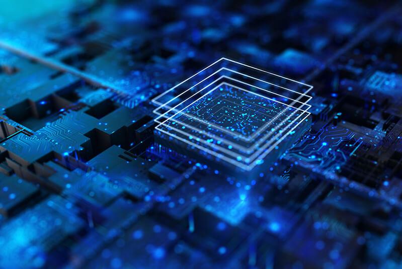
SI/PI simulation
SI/PI Simulation
In semiconductor test interface design, Chroma ATE uses SI/PI simulation as a key technology to ensure product performance stability.
- Signal Integrity (SI): Simulation is used to analyze issues such as distortion, reflection, and crosstalk during high-speed signal transmission, ensuring accurate data delivery.
- Power Integrity (PI): The simulation focuses on the stability of the power distribution network, reducing voltage fluctuations and noise interference.

Sstress-strainsSimulation
Stress-strain simulation
Engineering analysis technology is mainly used to study the mechanical behavior of materials or structures under external forces, especially their stress distribution and deformation. In semiconductor test interface design, we use stress-strain simulation to analyze the structural stability of probe cards under high pressure, elastic contact, or thermal expansion, optimizing the design to improve lifespan and performance.
This technology helps us accurately predict the ultimate load of probe materials, ensuring that various testing requirements are met under high reliability demands.
MMechanismstrainsSimulation
Organizational Contingency Simulation
Analyze the deformation behavior of mechanical structures or components under external loads. Through numerical simulation techniques, it is possible to predict the deformation, stress distribution, and potential failure locations of the structure under different stress conditions. In semiconductor test interface design, such simulations help analyze the structural stability of probe cards and test fixtures during high-pressure operation, ensuring their durability and performance, and optimizing the design to extend service life.
Thermalsimulation
Thermal simulation
The technology of using computer simulation to analyze and predict heat transfer and heat distribution of objects under different environmental conditions. It is widely used in product design, engineering development, and research to help engineers understand the thermal performance of products during the design phase and ensure their stability and efficiency in practical applications.
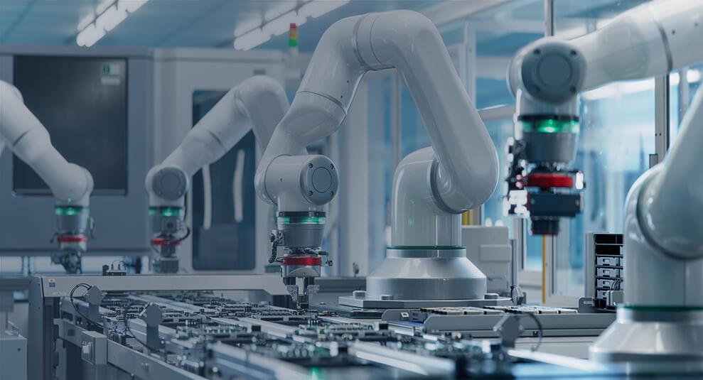
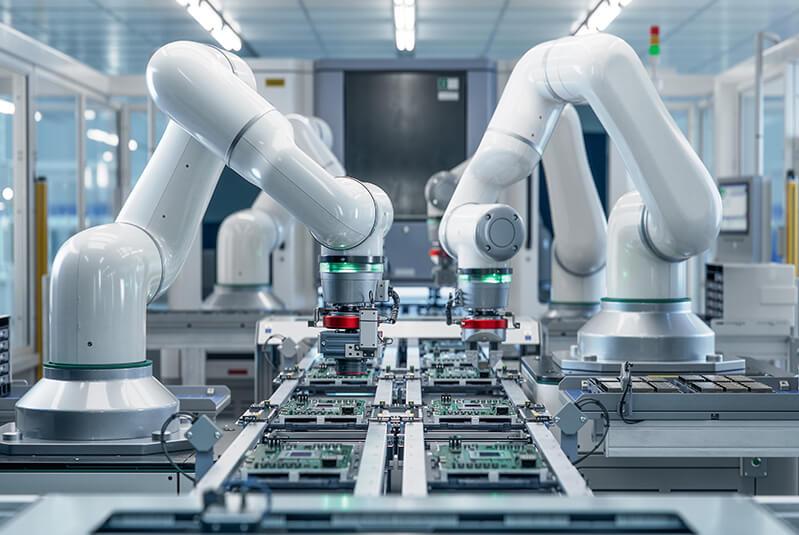
CHIP PROBING
Confirm that semiconductor components operate within the design specifications and eliminate chips that may have defects during the production process to avoid subsequent packaging.
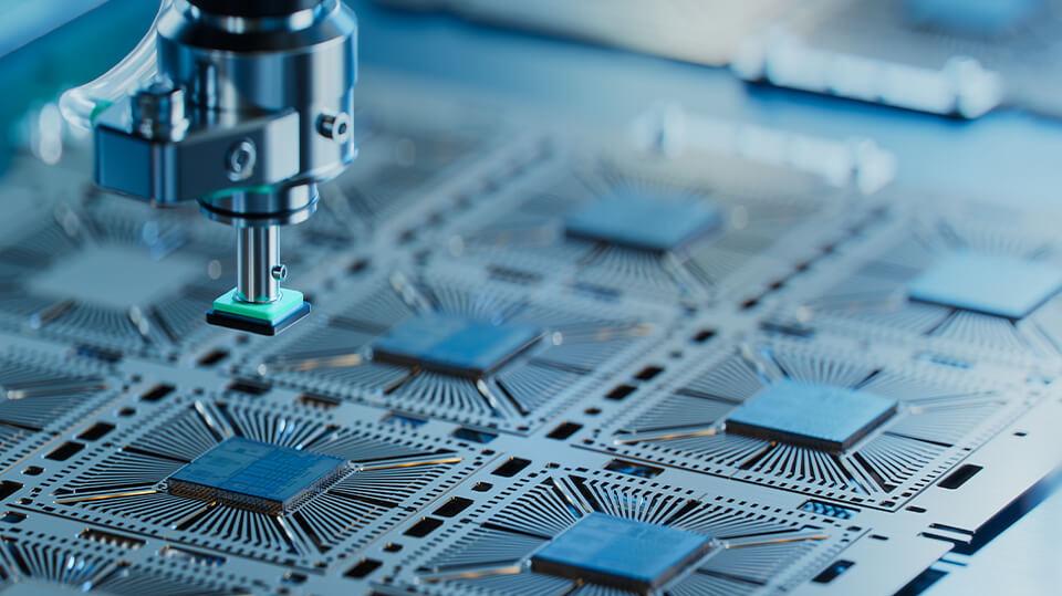
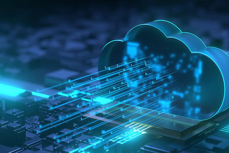
Final Test (FT)
It is an important test interface after IC packaging, mainly functioning as a carrier for the IC. When the wafer undergoes processes such as dicing, die bonding, and wire bonding, and is then encapsulated with materials like plastic, ceramic, or metal, the yield must be tested again.